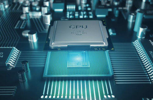
In the ever-evolving landscape of semiconductor technology, the rise of on-chip interconnect has emerged as a pivotal advancement, revolutionizing the design and functionality of modern microchips.
Understanding the Basics
Advanced packaging is highly complex and involves a wide mixture of technologies, interconnection technology remains at its core. At the forefront of this transformation are chiplets and Systems-on-Chips (SoCs).
First, it is important to note that interconnection technology is a critical and necessary part of packaging. Chips are interconnected through packaging to receive power, exchange signals, and, ultimately, operate. As the speed, density, and functions of a semiconductor product change depending on how the interconnection is made, interconnection methods are constantly changing and developing.
History
The evolution of interconnect technology can be divided into three distinct eras, The Buses, Crossbars and Network-on-Chip (NoC). The initial phase was characterized by the dominance of buses, where processors communicated with DRAM memory and other peripherals via read and write transactions over the bus.
As more initiators began to utilize the bus, the need for arbiters arose to manage access requests from various sources. During this period, numerous companies developed their own proprietary bus interconnect intellectual property (IP).
However, in 1996, a significant shift occurred with the introduction of the first widely accepted industry standard bus protocol for on-chip interconnects: ARM’s Advanced Microcontroller Bus Architecture (AMBA). This marked a pivotal moment in advancing IP core interoperability, allowing for greater standardization and compatibility across different systems and architectures.
In the 1990s, the integration of multiple cores within chips led to bus bottlenecks due to numerous initiators vying for access to different targets simultaneously, causing latency issues. To address this, crossbars emerged as a solution, enabling concurrent access and higher system data throughput by facilitating simultaneous communication between initiators and targets. However, as systems-on-chip expanded with more IP blocks, both buses and crossbars demonstrated limitations. Shared buses led to contention issues, while hierarchical designs of buses and crossbars increased system complexity.
Phase 3 introduced Network-on-Chip (NoC) technology, utilizing packet-based, serialized transmission to address wiring challenges. By consolidating address, control, and data information on the same wires, NoC reduces wire count while maintaining high-quality service. Distributing interconnect logic across the chip simplifies floor planning, and NoC offers a flexible balance between throughput and physical wire usage.
In today’s era, The open industry standard for die-to-die connectivity was introduced by a consortium of over 80 companies, including semiconductor and packaging firms, foundries, and cloud services and IP suppliers. It’s an important step toward heterogeneous integration with multidie systems and it’s aiming to create a new design ecosystem for semiconductor chiplets.
Among these the latest Bunch of Wire interconnect technology defines an open and interoperable physical interface between a pair of dies inside a single package. It specifies a physical layer (PHY) optimized for SoC disaggregation to form the basis of multi-die interconnect for chiplets.
This approach is expected to drive innovation in heterogeneous computing architectures, allowing for improved performance, flexibility, and cost-efficiency in future semiconductor systems.
More Information
https://semiengineering.com/a-brief-history-of-the-interconnect/https://www.prnewswire.com/news-releases/eliyan-applauds-release-of-ocps-latest-multi-die-openinterconnect- standard-bow-2-0-demonstrates-industrys-first-working-silicon-compliant-with-thespec- 301902004.html