Modern Day Designs
Technological advancements have touched and transformed almost every sphere of our lives. From the high-end satellites in space that give us accurate information on the weather, location, level of natural resources and a lot more to the smartphones in our hands, engineering marvels are ubiquitous. Cars in the olden days were merely machines running on fuel, but the modern day cars are equipped with computer vision and intelligence. When cell phones came into existence, they were hot and huge, but now the cell phones have shrunk and so have their power demands. Not to forget that our cell phones now even double up as a map, camera, audio-video player, notepad, watch, calendar and much more rolled into one. The lifelike sound and visual effects rendered by the modern day audio visual systems were unthinkable in the past. But as Rome wasn’t built in a day, the metamorphosis of almost everything we see and touch has taken years of research culminating into increasingly smarter designs.
The number of functions that a device is expected to carry out has increased and so has the complexity of the designs that make it possible. Moore’s Law continues to get validated. Hence as the number of transistors rises in the design, the struggle to innovate means for keeping the form factor and power consumption low looms large. The amount of money that now goes into one chip is in the tune of multi-million dollars and if the chip isn’t a success in the first spin, the money that goes into subsequent spins are astronomical too. It is very critical to ensure that the design works as per the specifications. Imagine the aftermath of a chip sitting in flight control systems or that in the ADAS (Advanced Driver Awareness Systems) going kaput for an instance!

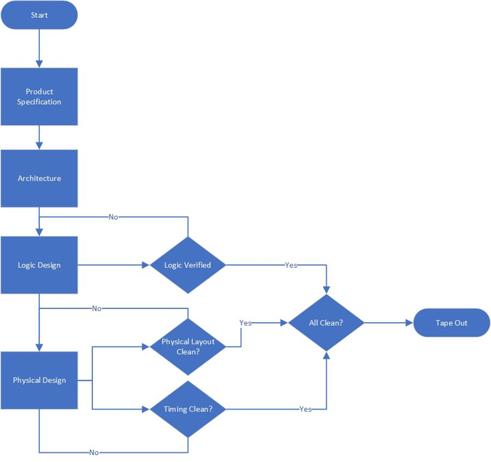
The above diagram depicts a typical ASIC cycle
What Is ASIC Verification?
What do we mean when we say the design is verified? It means that the design functions as per the specifications. But this is only one aspect of an ASIC verification cycle termed as ‘functional verification’. There is a lot more work that goes into ASIC verification, besides ensuring functional adherence. It is also imperative to ensure that the chip meets its timing and power consumption goals.
While designers are facing continuous pressure to squeeze in more features, verification engineers face the pressure to ensure none of those features is missed while verifying the chip. Designers invest time and energy in designing a chip that belts out multiple functions, fits the form factor, power consumption and timing specifications. While the verification engineering team burns the midnight oil to make sure that the chip does not consume more power than specified, the gate count does not exceed the specified one and the timing parameters are met, besides making sure that all the functions have been incorporated and functioning well. Functional verification can get quite daunting as the number of possible test scenarios even for simple design can be large. With the rise in design complexity, the number of test scenarios that would exercise each and every aspect of the code also rises. Besides coming up with a large number of test scenarios, verification engineers also must innovate ways to build smarter testbenches that are highly automated, reusable and accurate. As the chips get denser and faster, the task of reproducing ‘on-chip’ scenarios’ at the simulation level also gets more and more uphill. Chips that involve different clock domains or mixed-signals (both digital as well as analogue) can be quite challenging to verify for it is not easy to reproduce this in a simulation. It would be interesting if not surprising to note that 70% of the efforts in a typical ASIC cycle come from the chip verification team.

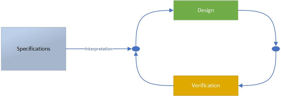
The above diagram depicts that Verification and Design begin in Parallel
When Do We Begin Verification?
It is easy to presume that the design phase begins as soon as the design specifications are laid out, while the verification process begins once the designers are done coding the design. On the contrary, the verification process runs in parallel with the design phase. Once the specifications are well understood by both the design and verification teams, both the teams spring simultaneously into action. The designers get busy preparing the higher level design architecture followed by the lower level implementation details. The coding begins after the design architecture has been thoroughly reviewed and agreed upon. On the other side of the fence, the verification team gets busy chalking out a higher level testbench architecture, followed by a detailed description of each and every testbench component. The development of test scenarios and testbench code begins only after the testbench architecture seems comprehensive to provide all possible stimuli required to exercise the design thoroughly.
Once the design verification begins, the interaction between the design and verification teams is established via the bug reporting and fixing channel. Verification is a lengthy process and verification engineers are expected to keep an eye for details. Apart from injecting ‘constrained random’ and ‘random’ stimuli into the design for a thorough functionality testing, the verification team must also prepare a suite of directed test cases. The directed test cases are usually aimed to cover those areas of the code that have not been exercised by randomization such as state machine or signal transitions that are difficult to cover. Directed tests may also be required to ensure that multiple clock domains and mixed-signal interfaces are functioning well. A lot of thought and effort goes before the verification manager announces a verification closure. Some of the metrics to decide this are the complexity and amount of bugs found and fixed, the coverage metrics, regression reports, gate level simulation results, etc.
Why Do We Need ASIC Verification?
ASIC (Application Specific Integrated Circuit) is designed for a fixed application, unlike an FPGA. An FPGA can play different roles depending on the design code programmed into it. It can also be reconfigured if there are design updates in the event of a bug fix. Sadly, none of this is possible in the case of an ASIC as the design code is hard wired into silicon. If there is a bug found post tapeout of an ASIC, a respin is inevitable. Each tapeout is very expensive and hence post tapeout bugs or the very idea of a respin is strong enough to knock the daylights off ASIC manufacturers.
Even if the design is a simple 4×1 MUX developing a cute little testbench around it and verifying different input-output combinations would help us gain confidence in what we designed, isn’t it? Won’t it be absolutely sensible to verify a design that is far more complicated than a simple mux? By listing out functionalities of the design and tracing test cases back to the feature it tested, we ensure that there can one or many scenarios that verify a feature and each scenario are linked to one or multiple features. By generating constrained random, random and directed stimuli and by tracking coverage metrics, it is ensured that each and every line of the code has been reached. By engaging scoreboards, monitors and protocol checkers one can be sure that data integrity has not been compromised and the protocol has not been violated at any point in time. Gate-level simulations render the confidence that the design can function in the given operating frequency range. With all the above-enlisted advantages and a lot more, ASIC verification is an ‘inevitable’ process.
Summary
The quest for smarter, faster and sleek looking gadgets is on a never-ending rise. Most industries that we see around are now largely driven by technology and this is just the beginning. Embedding microchips in human or animal bodies for diagnostic and research purposes respectively is no more a piece of fiction. With this kind of a pace of technology, the pressure on researchers and engineers across domains is rising. The concept of “less is more” is no longer applicable when it comes to applications/functions and hence more and more functions/logic is expected to squeeze into a design. However, this does not apply when one talks about power consumption and form factor as they are expected to steadily shrink.
Designing an ASIC is only 20-30% of the job done. The major chunk of work goes into verifying the design. ASIC verification is a process that ensures the design meets specifications. It commences as soon as the design specifications are laid out and runs in parallel with the design phase. Although it seems like a never-ending process, the complexity and frequency of bugs reported and fixed, coverage metrics, gate level simulation results and regressions reports are some of the essential parameters that serve as deciding factors to indicate verification closure. A single ASIC is worth a million dollars and it cannot be reconfigured in case a bug has been found post tapeout. Each subsequent tapeout is also expensive. The chips that sit into safety-critical applications such as in an aircraft or in a medical device or even for an instance a chip sitting inside our cellphone can prove detrimental towards human life. ASIC Verification thus can neither be substituted nor skipped as it holds a unique and irreplaceable significance in the ASIC cycle.