Layered architecture refers to a design methodology that divides the functionality of an integrated circuit (IC) into distinct layers, each responsible for a specific aspect of the design. This approach allows for better organization, abstraction, and modularity, making the design process more manageable and scalable. This also enables flexibility for design and implementation while retaining interoperability.
Advantages:
The layered architecture offers several advantages:
- Modularity: It allows the design to be divided into manageable modules or layers, each focusing on a specific aspect of the design.
- Abstraction: Each layer abstracts away implementation details, allowing designers to focus on higher-level functionalities without being bogged down by low-level details.
- Hierarchical Design: The layered architecture enables hierarchical design methodologies, where complex systems are built from simpler components. This hierarchical approach simplifies design complexity, improves design clarity, and enhances overall design comprehension.
- Ease of Debugging: Problems can be localized to specific layers, making debugging easier and more efficient. Designers can isolate issues within a particular layer without having to understand the entire system, speeding up the debugging process.
- Collaboration: Different teams can work on different layers simultaneously, promoting parallel development and collaboration leading to better coordination and faster design iterations.
- Scalability: The modular nature of the layered architecture makes it easier to scale designs to accommodate increasing complexity or changing requirements. New features or functionalities can be added by modifying or extending specific layers without affecting the entire design.
Overall, the layered architecture enhances productivity, facilitates design reuse, simplifies debugging, promotes collaboration, and enables scalability, making it an essential methodology in modern design processes.
ODSA Die-to-Die Interface:
A D2D interface is conceptually a layered architecture. The ODSA D2D interface defines the transaction, link and physical layers. The system interface, represented by the upper horizontal dashed line, is the boundary between the on-die interconnect and the transaction layer, while the link-physical interface (or LPI), represented by the lower horizontal dashed line, is the boundary between the link layer and the physical layer.
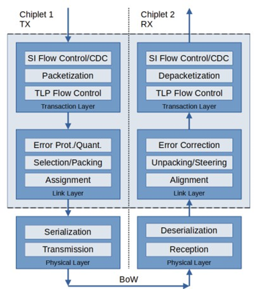
The following functions are performed by the Transaction Layer:
- CDC between the system interface clock domain and the BoW interface clock domain
- Packetize/Depacketize information received on the system interface into transaction layer packets (TLPs) and classify the TLPs into classes and streams
- Manage flow control for each stream with the far-side TX and RX interface.
The following functions are performed by the Link Layer:
- Add error-correcting code (SECDED) and quantize TLPs
- Correct single-bit errors and detect double-bit errors in TLPs
- Pack/Unpacking eligible TLPs from different TLP streams into link layer packets (LLPs)
- Assign/Align LLP fragments to PHY slice logic interfaces
The following functions are performed by the Physical Layer:
- Clock generation
- Serialization/Deserialization of fragments
- Transmit/Receive data from BoW interface
More Information:
- What is Layered architecture: https://cs.uwaterloo.ca/~m2nagapp/courses/CS446/1195/Arch_Design_Activity/Layered.pdf
- Layered Architecture – an overview: https://www.sciencedirect.com/topics/computer- science/layered-architecture
- Die-To-Die Chiplet Communication: https://semiengineering.com/die-to-die-chiplet-communication/