VeriSpark
Democratizing Access to Custom Silicon
In an era of heterogeneous compute and specialized Edge AI, standard off-the-shelf components often fail to meet specific Power, Performance, and Area (PPA) targets. VeriSpark is a comprehensive Custom Silicon Design Platform designed to bridge the chasm between architectural innovation and physical reality.
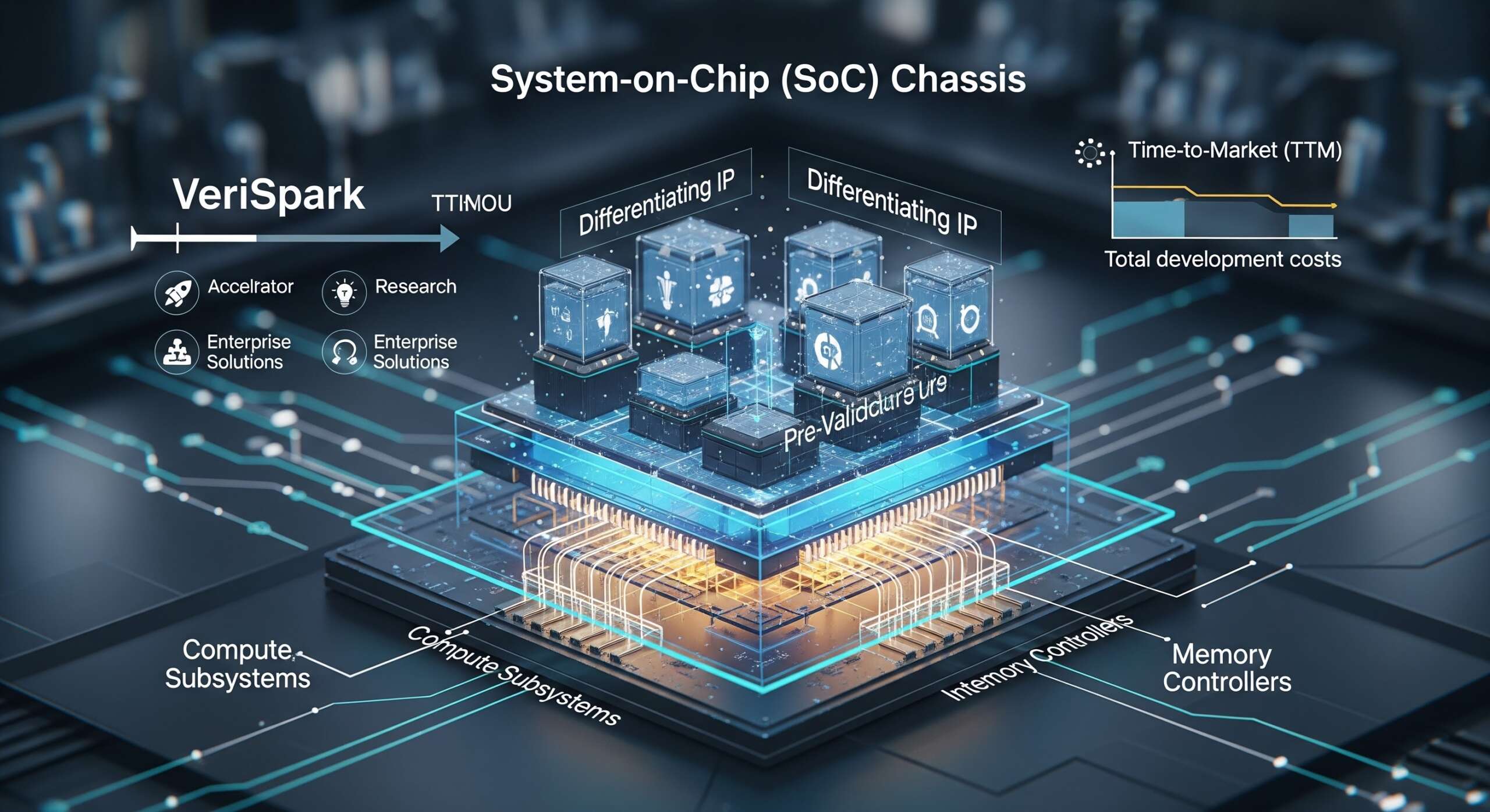
VeriSpark functions as a verified "System-on-Chip (SoC) Chassis," allowing you to bypass the high barriers to entry associated with semiconductor design. By providing a pre-validated infrastructure—including compute subsystems, interconnects, and memory controllers—VeriSpark enables startups, researchers, and enterprises to focus strictly on their differentiating IP. Whether you are aiming for low-volume production or validating a next-generation accelerator, VeriSpark slashes Time-to-Market (TTM) and total development costs.
Overview
A Modular, Foundry-Certified Architecture.
The VeriSpark architecture is built on a philosophy of flexibility and modularity, supporting a seamless “Plug & Play” silicon experience. It creates a robust foundation for custom SoC development through three core technical pillars:
- ISA Agnostic Compute: Future-proof your logic with a hybrid compute approach. VeriSpark supports industry-standard ARM cores (M, R, and A-Series) as well as the rapidly expanding open-standard RISC-V architecture (32-bit and 64-bit).
- Tiered Interconnect Fabrics: From simple AHB/APB bridges for microcontroller applications to high-bandwidth NoC (Network-on-Chip) and Cache Coherent Interconnects for application processing, the platform scales data movement capabilities to match your throughput requirements.
- Strategic Foundry Alignment: Developed in partnership with GlobalFoundries, the platform offers validated physical design pathways across three distinct technology nodes—GF180nm, GF22nm (FDX), and GF12nm (FinFET). This ensures that your design is not just a concept, but is manufacturing-ready for shuttle programs and launch tape-outs.
- Hybrid EDA Ecosystem: To further lower entry barriers, VeriSpark supports a dual-flow EDA environment, compatible with both cost-effective Open-Source tools and industry-standard Commercial design flows.
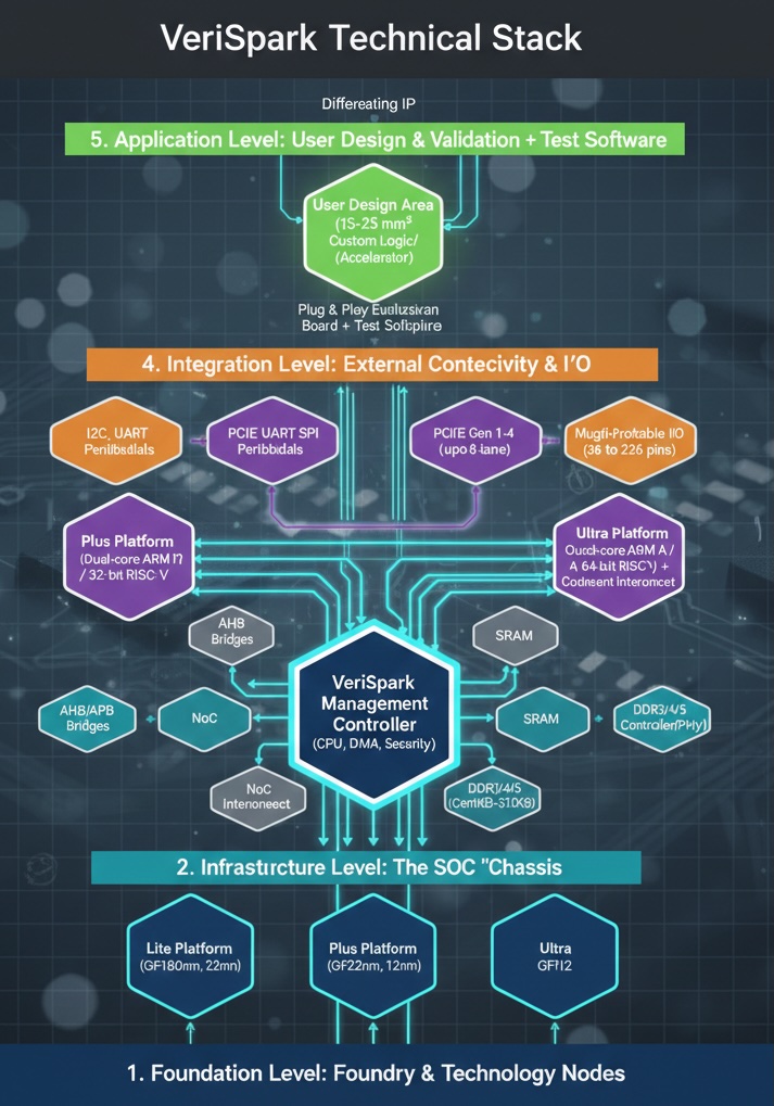

VeriSpark Lite: The IoT & Control Gateway
Compute: ARM M-Series or RISC-V Microcontroller.
Architecture: Features a Management Controller with an integrated DMA Engine and AHB/APB Bridge for efficient peripheral management.
Connectivity: 36-64 Configurable I/Os utilizing standard protocols (I2C, UART, SPI).
Packaging: Compact QFN100 package, portable to GF180 and GF22 nodes.
Unique Feature: Supports multiple design aggregations, allowing multiple distinct designs to share the same die area.
VeriSpark Plus: Real-Time Edge Processing
Compute: Dual-core ARM R-Series or RISC-V 32-bit Real-Time Controller.
Memory Sub-System: Advanced DDR Controller & PHY with 256KB On-Chip Memory (OCM) for data-intensive operations.
High-Speed I/O: Integrated PCIe Gen4 (up to x4 lanes) for high-bandwidth external connectivity.
Packaging: FCBGA-256 package, optimized for GF22 and GF12 technology nodes.
VeriSpark Ultra: High-Performance Application Node
Compute: Quad-core ARM A53 or RISC-V 64-bit Application Processor paired with a secondary real-time safety core.
Advanced Fabric: Utilizes a Cache Coherent Interconnect to maintain data consistency across heterogeneous processing units.
Maximum Connectivity: Supports up to PCIe Gen4 (x8 lanes) and Gigabit Ethernet (GigE).
Packaging: High-density FCBGA-576 package, exclusively designed for high-performance GF12 nodes.